

Transmission Line Tuning w/ HFSS
What is impedance matching
People often use the term “impedance matching” in corporate settings to mean basically anything they want. In the world of microwave and RF PCBA design it has a more specific definition.
Any transmission line along which an electromagnetic wave travels has a characteristic impedance (). This is basically the ratio of voltage to current for a wave travelling in one direction along the line. It can be engineered by changing the physical dimensions of the transmission line or the permittivity of the dielectric material that the wave travels in.
Here is why it matters: when there are changes in the impedance along the line, some of the incident wave will be reflected at the boundary.
This leads to two things you don’t want:
- The reflected wave interferes with the incident wave, making your clean bits smear together into something unrecognizable.
- Some of the power you wanted to deliver to your load no longer makes it.
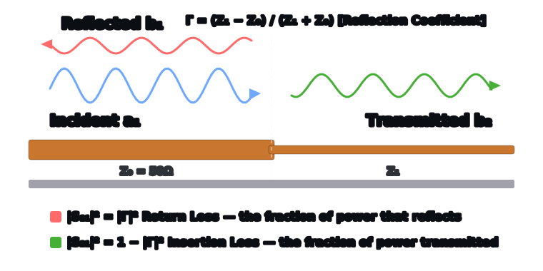
How to engineer it: For real microwave circuits a load impedance (e.g. antenna feed, transistor gate) different than your system impedance (almost always chosen to be 50Ω) is often unavoidable. When this happens you need to design a reactive matching network that uses inductors, capacitors, and transmission lines to transform your load impedance to appear as the system impedance over a narrow frequency band.
For transmission lines (and connectors) this is less necessary. For a transmission line the engineer generally gets to choose the dimensions to match their intended system impedance. Our goal here is to show how to engineer PCBA transmission lines and CPWG to a reflectionless 50Ω.
How to size PCBA transmission lines
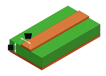
There are typically two ways to connect to a surface-mount RF component on a PCBA, microstrip or co-planar waveguide.
Microstrip is the simplest, but eliminates a degree-of-freedom in design. The characteristic impedance is a function of basically 3 things:
- : width of your trace
- : substrate thickness
- : The relative permittivity of your dielectric (substrate) material.
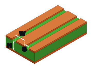
Coplanar waveguide with ground-plane (CPWG) adds a fourth degree-of-freedom.
- : Gap spacing between trace and top-copper ground plane
| Microstrip | CPWG |
|---|---|
 |  |
Here are some rule of thumb I use when thinking about transmission line sizing given .
| Relation | Why |
|---|---|
| then | Inner conductor width increases, distributed inductance decreases so characteristic impedance falls |
| then | Dielectric spacing increases, distributed capacitance decreases so characteristic impedance rises |
| then | Dielectric constant increases, distributed capacitance increases so characteristic impedance decreases |
Problem: In general, one should always aim for simplicity in design, and microstrip is simpler and has more-accurate closed-form equations for estimating its impedance. However, I often find myself getting stuck in the following rut.
- My substrate thickness is limited by common PCB fabricator stackups for affordability/manufacturability reasons (fewer layers reduces cost, PCBs are commonly 0.8mm-2.3mm for stiffness).
- Permittivity is determined by an outside core/prepreg vendor like Isola or Rogers.
- Trace width is limited by needing to enter/exit component footprints. For example, a QFN-24 footprint has 0.254mm (10mil) wide pads.
As an example: for a Rogers RO4350B PCBA built on a 2-layer 0.8mm (31mil) stackup, the Saturn PCB Toolkit (free) tells us that a 50Ω microstrip trace is 1.75mm wide. Obviously this doesn’t work as-is when trying to connect to a 0.254mm wide QFN pin.
CPWG as a solution: Often the solution to this sort of issue without adding more layers to the stackup is co-planar waveguide with a groundplane. This adds an additional free variable whose rule-of-thumb relation is the same as in the previous table.
| Relation | Why |
|---|---|
| then | Dielectric spacing increases, distributed capacitance decreases so characteristic impedance rises |
A real downside of CPWG however, is that the trace gap spacing required often turns out quite small; and PCB manufacturers can struggle with tolerancing and trace gaps smaller than 0.1mm.
Some readers will note that another drawback of CPWG (and Microstrip to a lesser extent) is that the signals do not propagate as strictly transverse EM mode. This means that at higher frequencies there can be mysterious overmoding problems. It also means that there are no analytic closed-form equations for characteristic impedance as a function of the CPWG dimensions. Instead approximate closed-form equations are fitted to measured results but this often leads to design equations that are significantly wrong. For this, a fancier simulation tool like ANSYS Electronics Desktop (a.k.a. HFSS) is needed.
Simulation with HFSS
In order to simulate our co-planar waveguide accurately. I used High Frequency Structure Simulator (HFSS) from ANSYS Electronics Desktop 2026 R1. Big thank you to Ketiv for helping Nine Fives get licensed via the ANSYS Startup program.
To set up our co-planar-waveguide in HFSS (High Frequency Structure Simulator) there are already two examples:
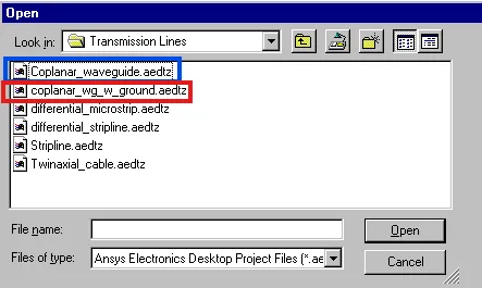
For reasons unknown, expanding the coplanar_wg_w_ground.aedtz leads ANSYS to crash, so I instead started with Coplanar_waveguide.aedtz.
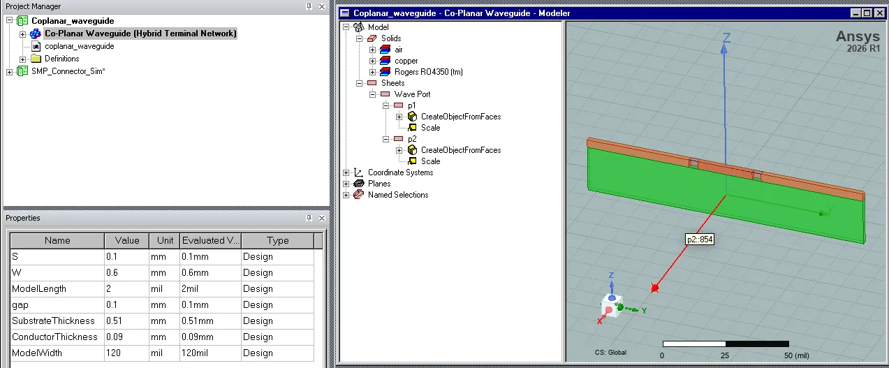
Some things to note:
- (Good) HFSS simulations tend to be heavily parameterized (see bottom left corner). This allows the designer to parametrically sweep variables as part of long-running simulations without manually redrawing everything.
- This specific simulation uses a very small model length (2mil). This means that the mesh is smaller and the simulation will tend to take less time. It also means any S-parameter plots (for mismatched lines) we generate won’t show periodicity in return loss, because the effective line length being so short means the period gets pushed to higher frequencies than we are likely to care about.
- This particular simulation has no stitching vias and no bottom ground. (It is CPW and not CPWG)
- The simulation is setup with Driven Terminal wave ports (these assume voltage and current, and therefore only support single mode simulation).
For the illustrative example I wanted to show on this page I changed a number of these assumptions:
- Changed simulation length to 10mm so we could see S-param periodicity at frequencies <10GHz with our velocity factor.
- Switched to Modal network (this is what I am used to, and it allows us to see multiple WG modes)
- Added a bottom ground plane. Used a real surface roughness model, added stitching vias and a perfect e-field boundary along the sides of the box.
Here’s what it looks like now:
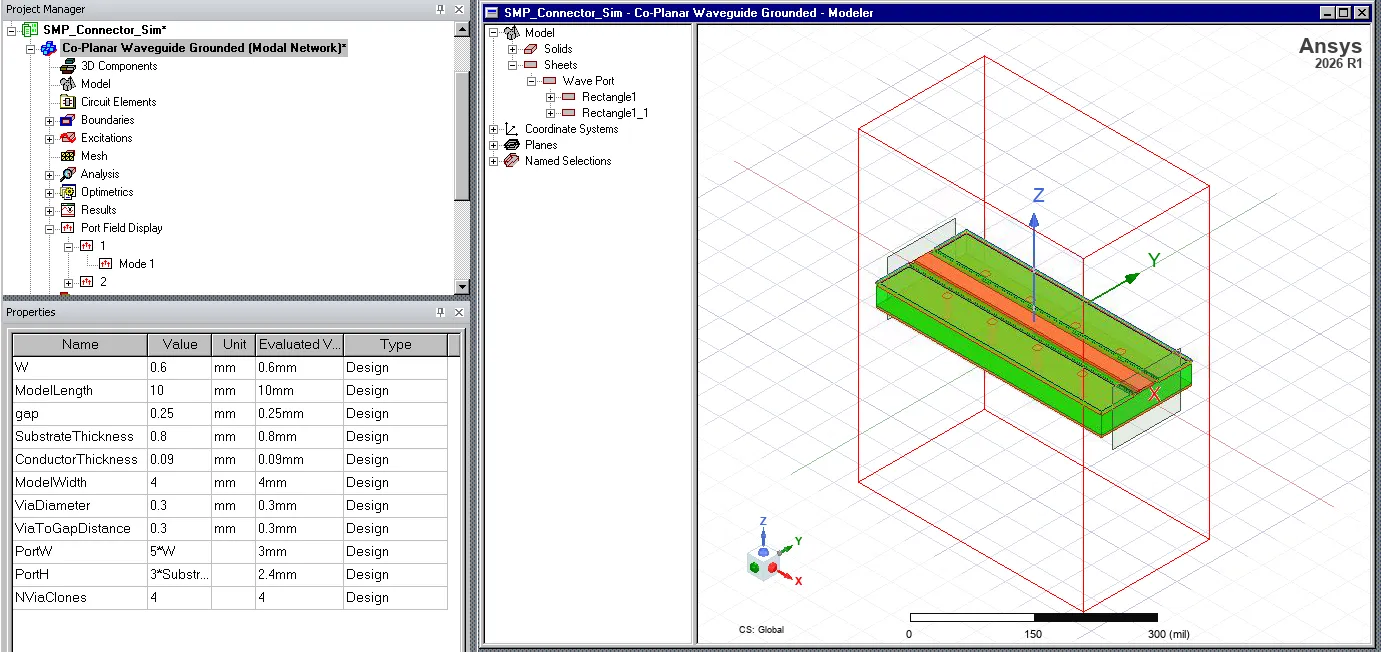
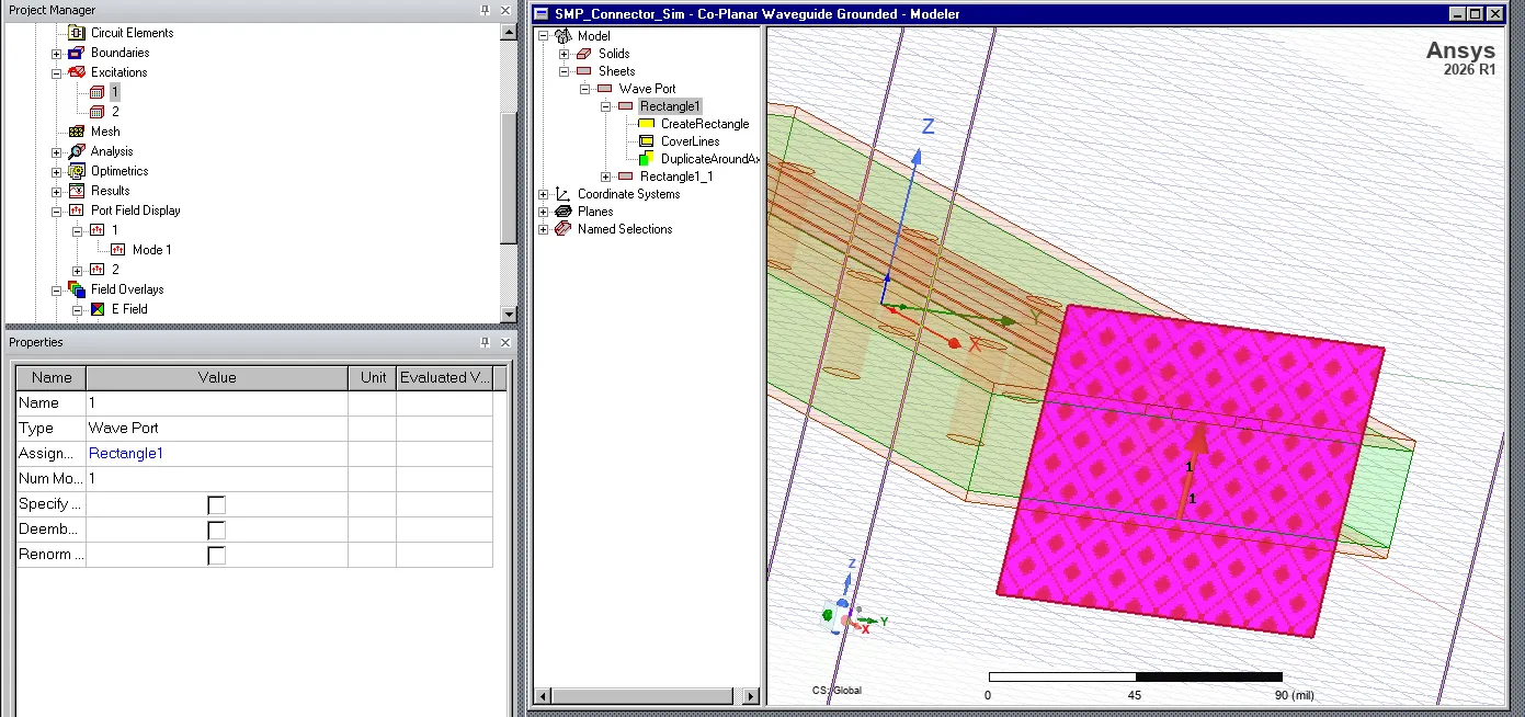
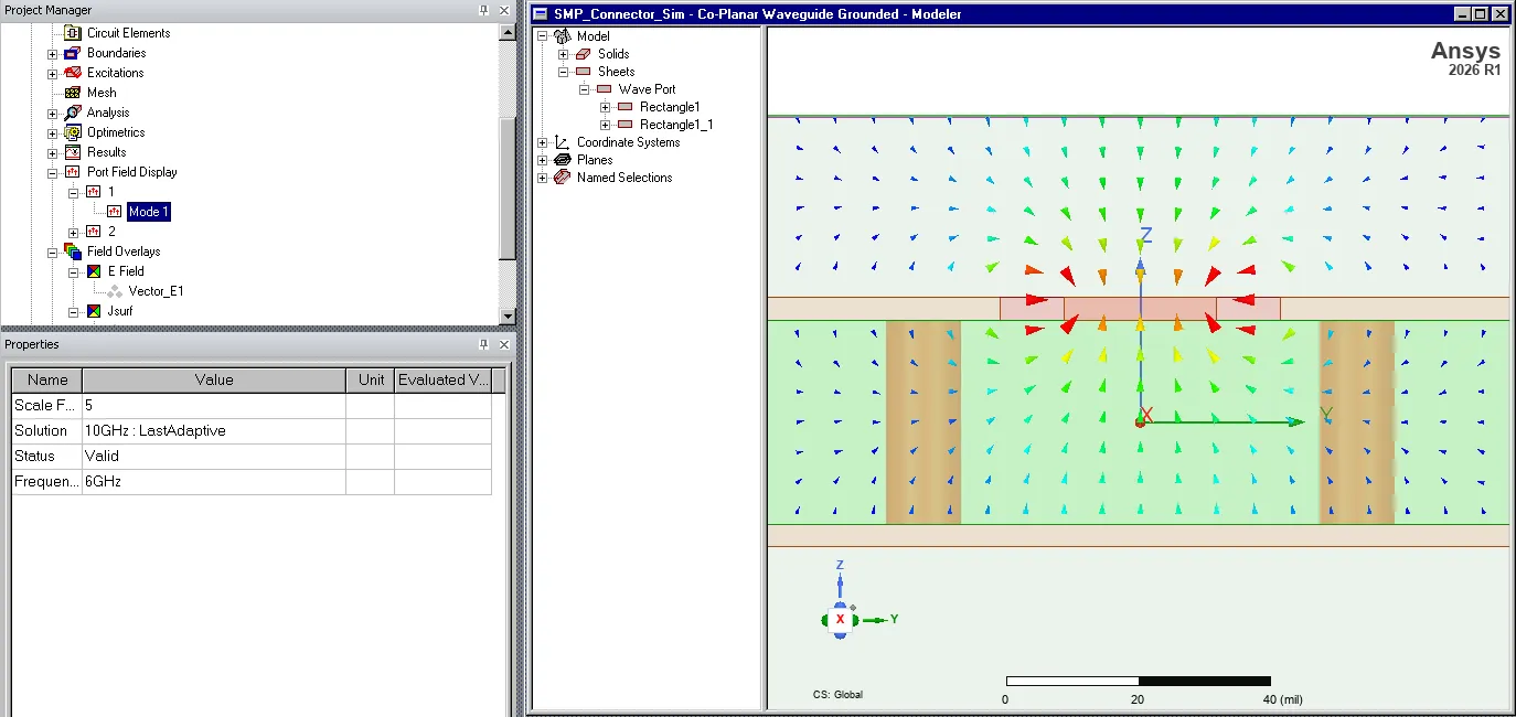
Wave ports can be tricky in HFSS. In general, the best way I have found to setup stuff correctly is to manually draw a line of integration that matches the E-field lines induced in the dielectric. For CPWG it is a bit odd because there will be field lines from the two side-ground conductors to the center conductor, as well as from the bottom conductor to the top conductor. I only drew the integration line from the bottom, and hoped that the structure would work to do the rest. Looking at the right image in this table, we can see that the strongest E-field lines (red) are from the side copper to the center conductor, with weaker field lines (cyan) pointing from the bottom ground to the bottom of the center conductor.
| Port integration line | Port E-field display |
|---|---|
 |  |
Sweeping the gap
With the port behaving, I can sweep the trace gap from 0.1mm to 0.35mm using HFSS optimetrics at a fixed tracewidth ().
This gives me a knob I can actually use to get a realizable 50Ω trace on a low cost, manufacturable RO4350B PCB.
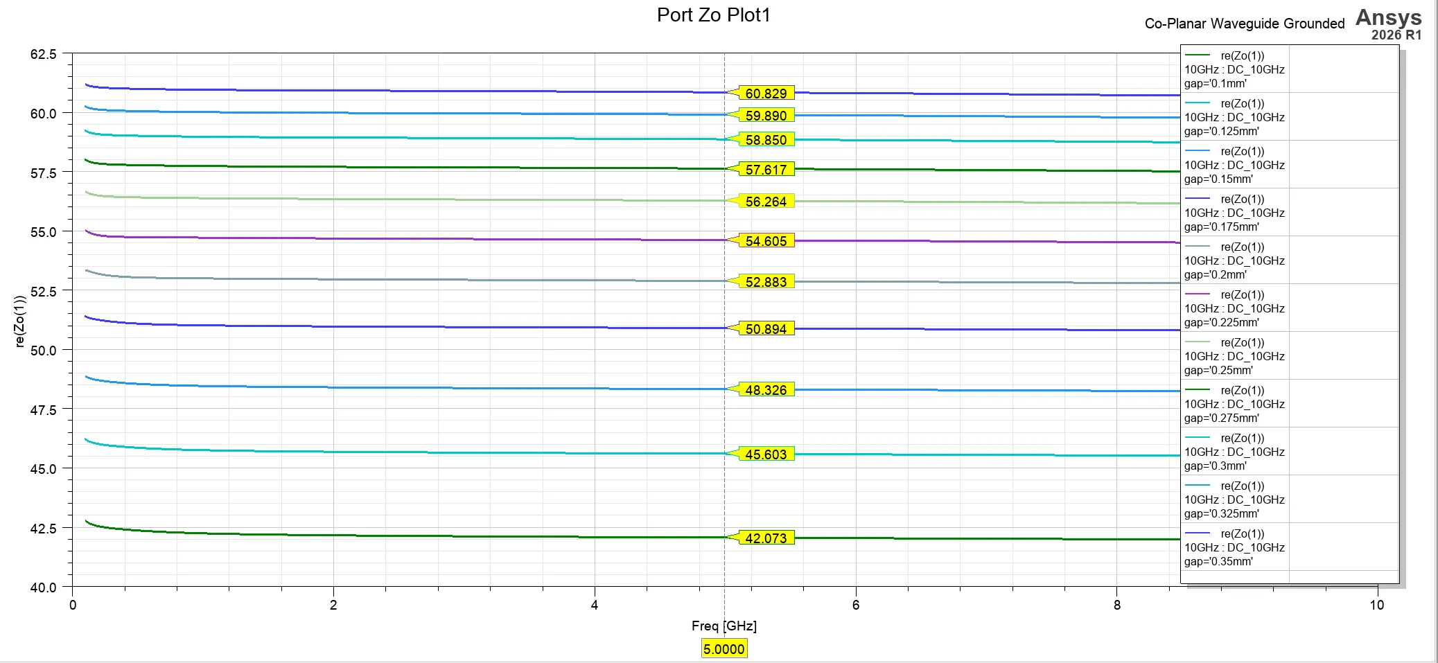
The impedance is basically flat across 100MHz–10GHz, so a single cut at 5GHz is enough to see the trend.
Closed-form equations vs. the simulation
Plotted alongside the HFSS data is the closed-form answer, from the quasi-static conformal mapping model that wcalc uses for CPWG. Each gap and the bottom ground plane contribute a partial capacitance, written as ratios of complete elliptic integrals :
The closed form equation runs 20–30% high across the whole sweep, and it is worst exactly where we want to operate. It wants less than a 0.1mm gap for 50Ω (likely unmanufacturable), where HFSS says 0.1mm actually gets you 42Ω. Trusting it would have you order a board with a harder-to-manufacture gap, only to give you worse results.
The main reason is that the equations assume zero metal thickness. Our copper (1oz + plating) is ~0.09mm thick. That extra sidewall area couples the trace to the coplanar grounds far more strongly than an infinitely thin conductor would, which pulls the impedance down. Wadell’s thickness correction claws most of it back at wide gaps, but it divides by the gap, so it degrades and then breaks down entirely right where the copper is as thick as the gap. Hence the 3D solver.
Return Loss (a.k.a S11)
When a wave travelling in a system of impedance hits a load , the fraction of the wave amplitude that bounces back is the reflection coefficient . Return loss is just that same number expressed in dB, and is what your simulator (or VNA) calls it when it is measured looking into port 1:
It is worth getting a feel for the scale. Our worst-case 0.1mm gap gave 42Ω into a 50Ω system:
So a mismatch this size is not a catastrophe on its own. It matters because is a voltage ratio that adds up over many discontinuities, and because — as we are about to see — the mismatch a source actually sees depends on how long the line is and what frequency you are at.
Periodicity in Return Loss along a mismatched line
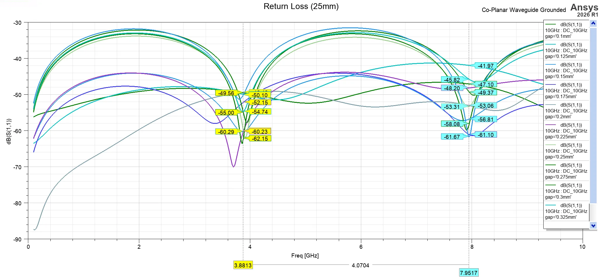
One way to understand the impact of a mismatched line, is to extend the simulated length to 25mm.
The velocity factor is a measure of the fraction of the speed of light that a signal propagates at through a medium (a.k.a. phase velocity ).
Things to keep in mind:
- When then
- so
For microstrip and coplanar waveguide, the effective permittivity is different than the true relative permittivity because some of the field lines are partially in air with .
The effective permittivity is just a weighted average of the two materials the field lives in. The weight is a filling factor : the fraction of the field that sits in the dielectric rather than in air.
For a coplanar line most of the energy is stored in the two gaps, and each gap is dielectric below and air above. So the napkin version is :
The input impedance of a mismatched, lossless transmission line is periodic every . For a 25mm line we can now solve:
So the transmission line should have no effect every (and should collapse) every ~3.9GHz: once near 3.9GHz, again near 7.8GHz, and so on. Our HFSS simulation basically matches this result; and the effect is much less pronounced for the transmission lines with impedances closer to , which shows us why we would want to design matched transmission lines in the first place.
Bonus visualization for fun
HFSS lets us plot the surface current magnitude along the various conductors as a function of incident port-phase. Practically speaking these plots aren’t super useful, but they can make for a fun visualization of “how” current travels in our circuit. Here is a visualization from HFSS of how our surface current magnitudes “travel” through the CPWG.