

How to vibecode a Wilkinson divider
TL;DR
LLMs can design basic microwave components if you give them the right tools, and it sped up my design process from a week to a day. The model wrote every schematic, simulation script and optimization loop below; my time went into prompting and reviewing its results.
Motivation
What separates Nine Fives from our competitors isn’t that we’re the only people that can design high reliability, performant RF circuits. Legacy vendors like Mini-Circuits, Pasternack, Fairview and others have been doing that for decades.
The problem comes when you need to integrate components from all these diverse vendors into a production test rack. Every vendor uses a different form factor and digital interface. Inevitably the production test rack becomes a spaghetti mess of coaxial cables and the test software becomes a series of kludges around different APIs, network topologies, and operating systems.
We solve this by offering a full catalog of RF test equipment that is compatible with our PD8X. Our active components, like POE-ATTEN-6G, POE-SPDT-6G, POE-SP4T-6G, are already the most modern and usable devices in the industry. But to really offer our customers an order-of-magnitude better experience than what exists today - we need to offer passive products in the same form factor, that support the same automatic device discovery via the PD8X chassis in our NineVue UI.
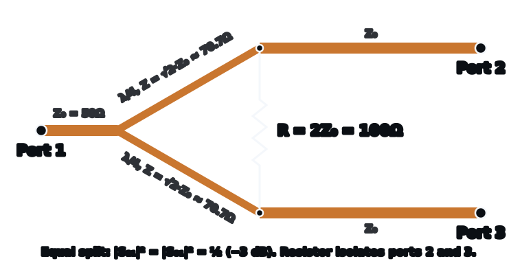
What is a Wilkinson Divider
The general idea of a Wilkinson divider is to create a matched, 3-port device whose S-parameter matrix (in dB) looks like
These circuits are useful because they allow for power injected into port 1 to be evenly split towards port 2 and port 3. Power injected into port 2 (or port 3) is “isolated” and only directed to port 1 (attenuated by 3dB). There are numerous ways Wilkinson dividers are used in RF test setups. A common example in a test environment might be to combine the outputs of a series of signal generators into the receive port of a DUT. This would (for example) let a drone company combine a jammer signal with an ExpressLRS command signal into their receiver’s U.FL port to test their drone’s tolerance to jamming.
Designing a Wilkinson divider is a pretty common task in RF design, and isn’t especially difficult, but it is the kind of task that LLMs were basically useless for until relatively recently. Seeing all the social-media gossip about the improved capabilities of recent models with CAD and electrical engineering, I decided to give LLMs a shot. I was pretty impressed with the results.
This is a high-level summary of the prompts and tools I used, not an exact copy-and-paste recreation.
Design Flow
In general for a lot of microwave circuits my design process is as follows.
- Gather requirements
- Find a relevant paper (or textbook section) for the circuit implementation.
- Create a model of the circuit implementation in a linear network simulator (typically Cadence AWR or Keysight ADS) based on the paper. — Tune it a bit to get the ideal sizing. Don’t over optimize here because everything will change later.
- Generate simplified artwork and simulate with a full-wave EM solver (HFSS, CST, or similar) — Tune design parametrically.
- Draw tuned design in real PCB software (KiCad, Altium, or similar)
- Export ODB++ or Gerbers and verify performance in HFSS.
Starting out
The real analysis tool for understanding how this circuit works [Even-Odd mode analysis] is covered in numerous places on the internet and in textbooks1,2 so I will ignore it here.
In the past I would have had to draw this circuit by hand using microstrip sections using Cadence Microwave Office or Keysight ADS. QUCS-S is an open-source network simulator that I have always regarded with suspicion, mostly because its user interface is quite rough around the edges. However for an LLM it might be the most approachable, because the schematic format is just text, and the simulator itself (qucsator_rf) can be invoked directly from the command line. As a result Opus 5.5 xHigh seems to have no trouble turning a relatively vague prompt into a well-formed linear simulation.
Opus wrote a python script that it used to generate the following schematic. Beyond placing the performance plots (not shown) on top of the note text and not using design variables, this is basically exactly the kind of schematic I would have made by hand as a line engineer in AWR or ADS in industry.
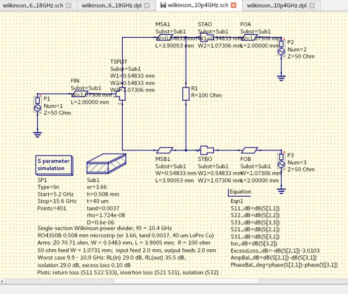
Some interesting stuff I never told it that it (evidently) figured out along the way.
- I never explained to it what a Wilkinson divider is. It correctly recognized I was referring to the structure in the diagram above, and figured out it needed to calculate:
- (width of a line)
- (width of a line)
- (length of a quarter-wave transmission line)
- In order to calculate these it needed to know the permittivity () of RO4350B and (for accurate losses) the . It entered those correctly in its QUCS-S schematic note in the lower left. A cool detail here is that I never asked it to document its work like this, but the documentation is useful.
Multi-Section Wilkinson
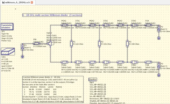
The above shows that Opus can generate a toy example of a Wilkinson divider with basically textbook performance. In reality, in order to achieve greater bandwidth Wilkinson dividers are normally multi-section affairs3. I decided to see if the LLM could do that:
Again, it generated a very reasonable QUCS-S schematic except for initially placing text labels and plots on top of the microstrip elements. One place it (arguably) could have done better is that it used all ideal resistors. At this stage in the design this isn’t unreasonable, but as we’ll see later, that can affect sizing a lot.
Simulating the layout using openEMS
Traditionally, once the rough network is figured out using closed-form models in AWR, ADS, or QUCS-S, the circuit then needs to be re-drawn by hand in a full-wave EM solver (AXIEM, Momentum, HFSS, or similar).
For this experiment, I initially wanted to use all free tools, so I attempted to use openEMS. I had never used openEMS before, due to hearing it was immature. Like QUCS-S though, it now occurs to me that (maybe?) the least mature part is the UI - which can be largely sidestepped by using an LLM.
Here’s the core of what it produced, wilkinson_6_18GHz_3d.py. This excerpt is the parameter block and the build() function, which constructs the whole
openEMS model. The rest of the script (not shown) is a small CLI that runs preview, run, and postprocess.
The LLM-generated openEMS script
Show code: wilkinson_6_18GHz_3d.py (excerpt)
# ----------------------------------------------------------------- parametersUNIT = 1e-3                      # all dimensions in mm
EPS_R = 3.66TAN_D = 0.0037H_SUB = 0.508                    # 20 mil coreT_CU = 40e-3                     # 40 um in mm (0.5 oz + plating)SIGMA_CU = 56e6
F_LO, F_HI = 6e9, 18e9F0 = 0.5 * (F_LO + F_HI)         # 12 GHzFC = 7e9                         # gaussian half-width -> 5..19 GHz
W_SEC = [0.320, 0.554, 0.823]    # section widthsL_SEC = [2.885, 3.877, 3.809]    # section lengthsR_ISO = [115.0, 191.0, 340.0]    # E96 isolation resistorsW_50 = 1.076                     # 50 ohm feed width
GAP = 0.8                        # arm inner-edge separation; resistor spanR_LEN = 0.30                     # resistor body length along x (0201-ish)TEE_LEN = 0.40                   # length of the common pad at the teeFEED_IN = 2.00                   # input 50 ohm stubFEED_OUT = 2.00                  # output 50 ohm stubs
MARGIN_X = 3.0                   # domain margin beyond metal (other variants)PORT_LEN = 3.5                   # MSL port: reference plane -> domain edgeFEED_SHIFT = 2.0                 # excitation plane, clear of the 8-cell PMLMARGIN_Y = 2.6AIR_Z = 4.0
RES_COARSE = 0.35                # ~lambda/25 at 18 GHz in eps_r 3.66RES_Y = 0.07                     # >=4 cells across the 0.320 mm sectionRES_X = 0.18                     # along the lines, where nothing is narrowMIN_CELL = 0.035                 # collapse grid lines closer than this
SIM_DIR = sim_dir('wilkinson_6_18GHz_3d')FREQ = np.linspace(F_LO, F_HI, 241)
# derived x stationsX_J = np.cumsum(L_SEC)                       # 2.885, 6.762, 10.571X_ARM0 = 0.0X_ARM1 = float(X_J[-1])X_TEE0 = -TEE_LENX_FEED0 = X_TEE0 - FEED_INX_OUT1 = X_ARM1 + FEED_OUT
Y_IN = GAP / 2.0                             # inner edge of each armY_TEE = Y_IN + W_SEC[0]                      # tee pad half-heightY_OUT = Y_IN + W_50                          # output stub outer edge
# x ends at the ports: only the MSL port line (launcher + PML) lies beyondX_MIN, X_MAX = round(X_FEED0 - PORT_LEN, 6), round(X_OUT1 + PORT_LEN, 6)Y_MAX = Y_OUT + MARGIN_Y

def _dedup(lines, protected, min_dist):    """Drop grid lines that all but coincide, keeping the important one.
    AddEdges2Grid places 1/3-2/3 lines wherever metal starts and stops. Those    land arbitrarily close to hand-placed filler lines, and two lines 0.7 um    apart make a cell that collapses the CFL timestep and blows the grading    ratio to 119. Nothing upstream removes them, so do it here: walk the    sorted lines and, whenever two sit closer than min_dist, keep the one that    is a real feature coordinate.    """    lines = np.unique(np.round(np.asarray(lines, dtype=float), 6))    prot = {round(float(v), 6) for v in protected}    out = []    for v in lines:        if out and (v - out[-1]) < min_dist:            if v in prot and out[-1] not in prot:                out[-1] = v            continue        out.append(v)    return np.array(out)

def _arm_boxes(sign):    """(lo, hi) pairs for one arm: sections, then the 50 ohm output stub."""    out = []    x0 = X_ARM0    for w, l in zip(W_SEC, L_SEC):        lo_y, hi_y = sorted((sign * Y_IN, sign * (Y_IN + w)))        out.append(([x0, lo_y, 0.0], [x0 + l, hi_y, 0.0]))        x0 += l    lo_y, hi_y = sorted((sign * Y_IN, sign * Y_OUT))    out.append(([X_ARM1, lo_y, 0.0], [X_OUT1, hi_y, 0.0]))    return out

def build(excite_port=1, lossy=False):    """Assemble the FDTD problem. Returns (FDTD, CSX, ports)."""    FDTD = openEMS(NrTS=60000, EndCriteria=1e-4)    FDTD.SetGaussExcite(F0, FC)    # ground plane is the zmin PEC boundary, as in the openEMS MSL tutorials    FDTD.SetBoundaryCond(['PML_8', 'PML_8', 'PML_8', 'PML_8', 'PEC', 'PML_8'])
    CSX = ContinuousStructure()    FDTD.SetCSX(CSX)    mesh = CSX.GetGrid()    mesh.SetDeltaUnit(UNIT)
    # ---- substrate (priority 0; every metal must outrank it) ----    kappa = 2 * np.pi * F0 * EPS0 * EPS_R * TAN_D    sub = CSX.AddMaterial('RO4350B', epsilon=EPS_R, kappa=kappa)    sub.AddBox([X_MIN, -Y_MAX, -H_SUB], [X_MAX, Y_MAX, 0.0], priority=0)
    # ---- top copper ----    # PEC while checking geometry: a conducting sheet is simulated but never    # appears in openEMS' PEC debug dump, so the preview would render blank.    if lossy:        metal = CSX.AddConductingSheet('cu', conductivity=SIGMA_CU,                                       thickness=T_CU * UNIT)    else:        metal = CSX.AddMetal('cu')
    metal.AddBox([X_FEED0, -W_50 / 2, 0.0], [X_TEE0, W_50 / 2, 0.0],                 priority=10)                                    # input stub    metal.AddBox([X_TEE0, -Y_TEE, 0.0], [X_ARM0, Y_TEE, 0.0],                 priority=10)                                    # tee pad    for sign in (+1, -1):        for lo, hi in _arm_boxes(sign):            metal.AddBox(lo, hi, priority=10)
    # ---- isolation resistors, straddling each section junction ----    for i, (xj, r) in enumerate(zip(X_J, R_ISO), start=1):        res = CSX.AddLumpedElement(f'R{i}_{r:.0f}R', ny='y', caps=True, R=r)        res.AddBox([xj - R_LEN / 2, -Y_IN, 0.0],                   [xj + R_LEN / 2, Y_IN, 0.0], priority=20)
    # ---- mesh ----    # Metal edges go exactly on grid lines rather than using the 1/3-2/3 rule    # via AddEdges2Grid. The edge rule is more accurate at a field    # singularity, but here it drops lines a few microns from the fill lines    # and the grading ratio blows out to 5-119x, which reflects far more    # energy than the edge treatment recovers. Exact edges also keep the    # synthesised trace widths exact instead of snapping them.    x_feat = [X_MIN, X_FEED0, X_TEE0, X_ARM0, X_ARM1, X_OUT1, X_MAX]    x_feat += [float(v) for v in X_J]    x_feat += [float(v) for xj in X_J for v in (xj - R_LEN / 2, xj + R_LEN / 2)]    mesh.AddLine('x', np.round(x_feat, 6))
    y_feat = [0.0, Y_MAX, -Y_MAX]    for w in W_SEC + [W_50]:        y_feat += [Y_IN + w, -(Y_IN + w)]    y_feat += [Y_IN, -Y_IN, W_50 / 2, -W_50 / 2, Y_TEE, -Y_TEE]    mesh.AddLine('y', np.round(y_feat, 6))
    # substrate: 5 cells through the 0.508 mm core; then graded air above    z = [np.linspace(-H_SUB, 0.0, 6)]    zz, step = 0.0, 0.10    air = []    while zz < AIR_Z:        zz += step        step = min(step * 1.35, RES_COARSE)        air.append(zz)    z.append(np.array(air))    mesh.AddLine('z', np.round(np.concatenate(z), 6))
    # Only feature coordinates are placed by hand; SmoothMeshLines subdivides    # each interval between them. Adding a uniform fill on top of the features    # is what produced the 4.4x grading: a 36 um sliver wherever a trace edge    # happened to land just short of a fill line.    protected = {'x': x_feat, 'y': y_feat, 'z': [-H_SUB, 0.0]}    res = {'x': RES_X, 'y': RES_Y, 'z': RES_COARSE}    for i, d in enumerate('xyz'):        mesh.SetLines(d, _dedup(mesh.GetLines(i), protected[d], MIN_CELL))        mesh.SmoothMeshLines(d, res[d], 1.3)
    # ---- ports: 1 = input, 2 = +y output, 3 = -y output ----    # MSL ports place their probes on existing grid lines, so they go in after    # the mesh is final. Each box runs inward from the domain edge (feed end)    # to the reference plane and draws its own strip. The stubs above stop at    # the reference plane, so there are no duplicate boxes ("Unused    # primitive"). MeasPlaneShift = PORT_LEN puts the V probe on the    # reference plane itself, so no de-embedding is needed.    ports = []    specs = [(X_MIN, X_FEED0, -W_50 / 2, W_50 / 2),             (X_MAX, X_OUT1, Y_IN, Y_OUT),             (X_MAX, X_OUT1, -Y_OUT, -Y_IN)]    for nr, (x_edge, x_ref, ylo, yhi) in enumerate(specs, start=1):        ports.append(FDTD.AddMSLPort(            nr, metal, [x_edge, ylo, 0.0], [x_ref, yhi, -H_SUB], 'x', 'z',            excite=1.0 if nr == excite_port else 0.0,            FeedShift=FEED_SHIFT, MeasPlaneShift=PORT_LEN, priority=30))
return FDTD, CSX, ports- Parameters. Everything is in mm (
UNIT = 1e-3). The substrate constants and the section widths/lengths (W_SEC,L_SEC) come straight from the QUCS-S synthesis. The isolation resistors (R_ISO) are already rounded to E96 values. Then come the layout choices the schematic never had to make: the gap between the arms (GAP = 0.8, which is also the resistor span) and the lengths of the input/output feed stubs. One miss:R_LEN = 0.30is closer to an 0201 than the 0402 I asked for (its own comment says “0201-ish”). The later semi-circular layouts use the real Vishay FC terminal gaps. - Stations.
X_J = np.cumsum(L_SEC)gives the x position of each section junction, which is where the resistors go. The arms are inner-edge aligned: the inner edge of each arm stays at for the whole length, so the width steps happen on the outer edge and all three resistors span exactly the same gap. - Solver setup.
SetGaussExcite(F0, FC)puts a Gaussian pulse centered at 12 GHz with enough spectrum to cover roughly 5–19 GHz. The boundaries are PML on every side except , which is a PEC wall that doubles as the L2 ground plane (the same trick the openEMS microstrip tutorials use). - Substrate. RO4350B is a single dielectric box. openEMS wants loss as a conductivity rather than , so it converts one to the other at the center frequency: .
- Copper. The traces are zero-thickness boxes at : input stub, a small tee pad, then three sections plus a 50 Ω output stub per arm (
_arm_boxes). For real runs they’re a lossyConductingSheet(copper conductivity and thickness); for geometry previews they’re plain PEC, because conducting sheets don’t show up in openEMS’ debug dump. - Resistors. Each isolation resistor is an openEMS
LumpedElementoriented along y, bridging the gap between the arms at a section junction. - Ports. All three ports are 50 Ω microstrip (MSL) ports. Each one continues its 50 Ω stub straight out through the domain edge into the PML, which makes
the line look infinitely long and matched, the openEMS equivalent of an HFSS wave port on a trimmed air box. The domain in x ends there (
PORT_LENpast each reference plane). The excitation sitsFEED_SHIFTin from the edge, clear of the PML, and the voltage/current probes sit on the reference planes, so nothing needs de-embedding. The first version used lumped ports instead. Those left a −25.5 dB floor in a thru-line calibration check, which the MSL ports remove. There’s one catch: the two output lines stay 0.8 mm apart all the way into the PML, so they form a coupled pair and neither is terminated in exactly 50 Ω.postprocesshandles this by measuring the incident and reflected waves at every port for every excitation and solving for the full S-matrix. - Mesh. This is where most of the iteration went. It puts grid lines exactly on every metal edge and resistor end rather than using the usual
1/3–2/3 edge rule, runs 5 cells through the substrate, and grades the air cells above. Then
_dedupdeletes grid lines that sit almost on top of each other, andSmoothMeshLinesfills in between them. The comments say what went wrong first: lines micrometers apart wrecked the timestep and pushed the cell-to-cell grading ratio as high as 119×.
What does the LLM-generated openEMS routing actually look like?
A note for HFSS users: the ports don’t sit on the edge of the air box. In HFSS a wave port is a boundary condition solved on the outer face, so it needs no length. openEMS is an FDTD solver, and its PML absorber lives inside the mesh (here the outer 8 cells, about 1.4 mm in x). So each port is a short length of 50 Ω line that runs into the PML, which makes it look infinitely long and matched. The excitation (red) sits just inside the PML, and the voltage/current probes (blue) sit further in, at the reference plane where the S-parameters are measured.
openEMS results vs. QUCS-S
The plots in this post run from 10 MHz to 20 GHz, with the 6–18 GHz spec band shaded. For the openEMS curves the pulse was widened to cover DC–24 GHz
(WILK_FREQ=0.01,20,2000 in the script) instead of the 5–19 GHz excitation above.
The two simulations agree well on insertion loss, but openEMS shows worse isolation and input match at the top of the band. This is most likely due to inter-line coupling. The QUCS-S schematic treats each arm as an independent transmission line, but in this layout the two arms run parallel only 0.8 mm apart for their whole length, so they behave like a coupled pair, and the coupling gets stronger as frequency goes up. This is why Wilkinson dividers are so often drawn with semi-circular (ring-shaped) sections. Curving the arms away from each other keeps them far apart along most of their length, and they only come close at the points where the isolation resistors need to bridge them.
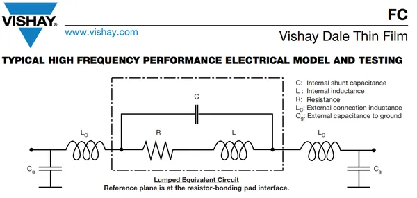
Using a real resistor model
Normally, the next step would be to run iterative optimization within the EM solver to find a topology with arced microstrip segments that hits the same transmission line impedances and lengths - this can be pretty time consuming so we should first make sure that our linear circuit is right.
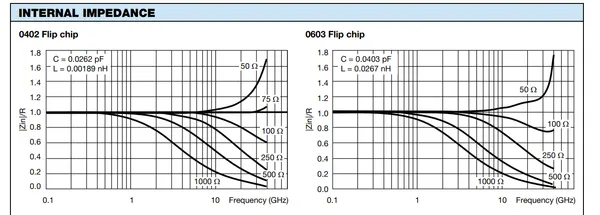
The isolation resistors in the Wilkinson divider are actually significantly non-ideal. For thin-film flip-chip resistors (commonly used at microwave frequencies) the datasheets will give an RLC model. Here I am using the Vishay FC series: https://www.vishay.com/docs/60093/fcseries.pdf.
Optimizing with openEMS
Full disclosure here: there was significantly more back and forth than I have shown. I encouraged the LLM to use MSL ports, and used the LLM to evaluate options using both 0402 and 0603 Vishay flip-chip resistors.
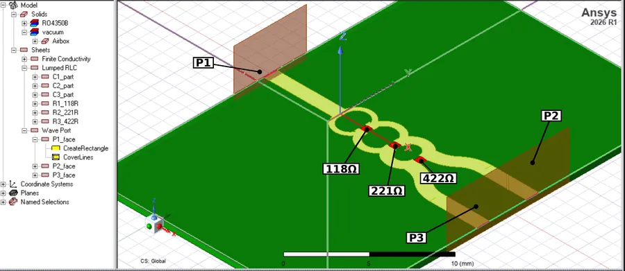
Using Ansys EDT (HFSS) to verify the passing semi-circular design
The 0603 version passed in openEMS but not in HFSS: excess loss came out at 0.67 dB against the 0.5 dB limit. When the LLM dug into it, about 0.16 dB of the difference was the openEMS ports under-reading loss, and most of what was left was radiation from the bends. The 0603’s 0.864 mm terminal gap and larger lands were part of that, so I had it run the same flow again with the Vishay FC0402 flip chip, whose terminal gap is 0.559 mm. That one passes in both solvers.
Each arm of each section is a semicircle. Neighboring arcs share an endpoint on the edge of the 0.559 mm gap between the resistor terminals, so the two arms of a section close into a full circle and every resistor bridges the same gap. The LLM ran a Nelder–Mead search directly on openEMS, about two minutes per evaluation. It varied each section’s arc length and width, R2, R3 and the output bend, and scored every candidate against both the raw openEMS curves and an HFSS-corrected version of them. A candidate only counted if it was predicted to pass in both. The resistors were snapped to E96 at the end, and the final layout was solved again in openEMS and HFSS.
| Section | W (mm) | Arc length (mm) | Radius (mm) | R (Ω, E96) |
|---|---|---|---|---|
| 1 | 0.351 | 3.444 | 1.096 | 118 |
| 2 | 0.515 | 3.782 | 1.204 | 221 |
| 3 | 0.797 | 3.387 | 1.078 | 422 |
The QUCS-S curve is the FC0402 re-tuned circuit the search started from. The openEMS and HFSS curves are the tuned semi-circular layout. Worst case across the band:
| QUCS-S circuit | openEMS | HFSS | Spec | |
|---|---|---|---|---|
| Isolation | 23.4 dB | 21.1 dB | 20.5 dB | ≥ 20 dB |
| Excess loss | 0.27 dB | 0.24 dB | 0.48 dB | ≤ 0.5 dB |
| Input return loss | 22.9 dB | 17.9 dB | 15.4 dB | — |
| Output return loss | 22.9 dB | 22.5 dB | 20.6 dB | — |
It meets the spec in both solvers. Phase balance is within 0.05° in both, against the 3° limit (expected, since the layout is mirror-symmetric). openEMS showing less loss than the circuit is the same port error as before, not a better layout. The margins in HFSS are thin, though: 0.5 dB on isolation, at about 11 GHz, and only 0.017 dB on excess loss, at 18 GHz.
That loss margin is worth putting in context.
- HFSS’s wave ports add about 0.03 dB of their own at 18 GHz, so the real loss is probably closer to 0.45 dB.
- On the other hand, the model uses smooth copper and a perfect ground. ENIG plating, copper roughness, the real pad and solder geometry, and etch tolerance would each add some loss.
So this is a design that passes in simulation, not one I’d send to fab without another pass.
Conclusion
LLMs (or at least Opus 5.5) are a lot more capable at basic microwave design work than they were a few months ago. They also significantly level the playing field between open-source tools (like QUCS-S and openEMS) and the industry-standard closed-source tools like Microwave Office, Keysight ADS, ANSYS Electronics Desktop (HFSS). QUCS-S’s text-format schematics and command-line simulator (qucsator_rf) help it overcome its UI deficiencies when it comes to getting work done with LLMs. It is a very exciting time to be building in this industry.
This divider is part of our push to bring passive components into the same form factor, and the same automatic discovery in NineVue, as our PD8X-compatible attenuators and switches. To see the programmable RF test equipment available today, visit ninefives.com.
Footnotes
-
E. J. Wilkinson, “An N-Way Hybrid Power Divider,” IRE Trans. Microwave Theory and Techniques, vol. 8, no. 1, pp. 116–118, Jan. 1960. ↩
-
D. M. Pozar, Microwave Engineering, 4th ed. Wiley, 2011, Sec. 7.3. ↩
-
S. B. Cohn, “A Class of Broadband Three-Port TEM-Mode Hybrids,” IEEE Trans. Microwave Theory and Techniques, vol. 16, no. 2, pp. 110–116, Feb. 1968. ↩